Board renders
Your board, photographed
before it exists.
Drop in the STEP file your CAD tool exported, or just the Gerbers. Either comes back as a render — real materials, real lighting, the board lit like a product shot rather than a viewport screenshot. Send both and you get the parts from one and the copper, mask and legend from the other.
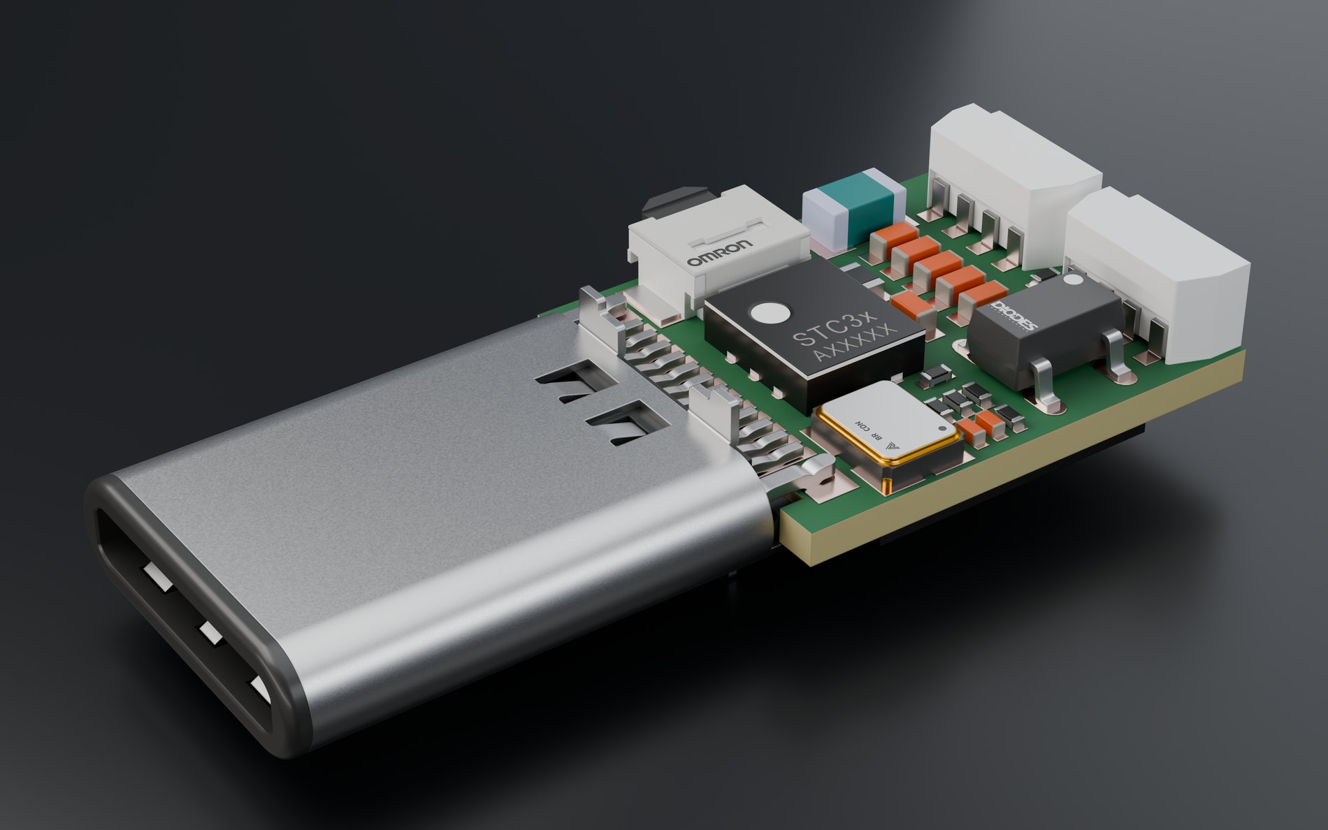
Either one alone is enough, and both together is the best of it: the assembly supplies the parts and the board's real thickness, the Gerbers supply the outline, copper, soldermask and silkscreen. Free while we tune it.
Sending a confidential design? Zip only your top layers — top copper, top soldermask, top silkscreen and the board outline. That is genuinely all a picture of a board is made of; your inner layers, your stackup and your netlist tell the renderer nothing it can draw with, so leave them out. Just remember your vias — the drill file is what puts the holes in the board, and without it you get back a clean, convincing, completely undrilled render.
What you get back
From the STEP alone
The assembly exactly as exported — components, connectors, mechanical parts, board outline. Whatever copper the STEP already carried is what you see.
With the Gerbers
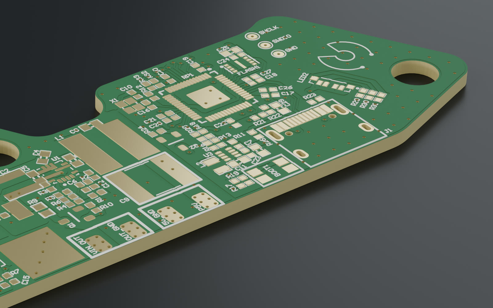
The copper is rebuilt onto the board from the layers themselves, so traces, pours, soldermask and silkscreen are the ones going to the fab. They render on their own as well as over an assembly.
Both together
The STEP is the base and the Gerbers are the detail printed onto it. The board's real thickness is measured off the assembly rather than assumed — Gerbers do not carry it — and the outline, copper, mask and legend come from the layers. Your 2.2 mm board renders 2.2 mm thick.
Legend like printed ink
Silkscreen is built as the bead it is: screen-printed wet and pulled round by surface tension, so it sits proud of the mask with a rounded shoulder and catches a highlight along its crown — not a flat decal.
Path-traced, not previewed
Real hardware and a real light transport solve: 4480×2800 at 256 samples, with the CAD tessellated fine enough that a pin is round rather than a polygon. That is why it reads as a photograph of a board instead of a screenshot of one.
We never save your files
Your STEP and your Gerbers are read, rendered and dropped. Partly principle, mostly that we are far too broke to afford the storage — there is no archive here to leak because we could never have afforded the archive. If your security review wants every cached file held on a ramdisk so nothing touches a disk at all, say so and we will set it up.
Working in a format we do not read yet? Tell us which one and we will add it — that is usually a 24-hour turnaround, not a roadmap item. Ask for a format →